- Quantum Chemistry / DFT
- Optical / Electrical / Magnetic
- Materials Science
[Analysis Example] Analysis example of semiconductor band gap correction by LDA+U method
Analysis of semiconductor band structure with high accuracy using SIESTA
Power semiconductors are widely used in switching devices and inverters for high-voltage and high-current applications in power systems and have high withstand voltage characteristics. The voltage holding capability of semiconductors is determined by the size of the band gap that separates the valence band from the conduction band. Power semiconductors are also called wide-gap semiconductors because they have a gap that is three times wider than the band gap of Si and GaAs. Therefore, material design using semiconductors by simulation assumes that the band gap can be estimated accurately, but the ab-initio calculations based on density functional theory (DFT) predict a much smaller gap than experimental results, depending on the target (Figure 1).
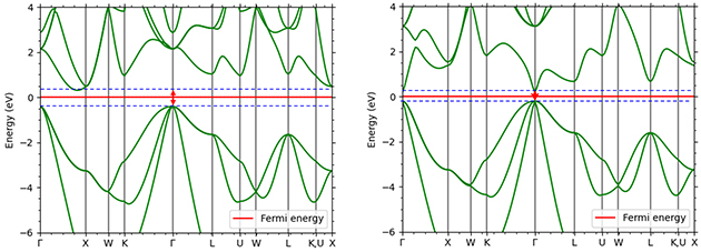 Figure 1. band calculation results of semiconductors by GGA method (left Si/right GaAs)
The band gap magnitudes calculated by the uncorrected GGA method are 0.72 eV for Si (experimental value 1.12 eV) and 0.37 eV for GaAs (experimental value 1.42 eV). These results are almost identical to the predictions given by the general uncorrected DFT.
It is known that this is due to the excessive delocalization of electrons by the density functional method [1][2], and one method that improves this drawback is the LDA+U method [3].
In the LDA+U method, when two electrons in the applied orbitals come to the same site, they are repelled and their energy increases by U. As a result, the excessive delocalization of electrons is suppressed and the band structure is restored.
In this case study, the LDA+U method was applied to analyze the band gaps of Si and 4H-SiC (indirect transition semiconductors) and GaAs and GaN (direct transition semiconductors).
For all semiconductors, the LDA+U method is applied to the p orbitals constituting the valence band. 3p orbitals are targeted for Si, but since the other three semiconductors are compound semiconductors, it is necessary to select an element with a p orbital constituting the valence band. Here we focus on the difference in electronegativity of each element: in GaAs, As has greater electronegativity, and electrons in the 4p orbital of Ga are attracted to the 4p orbital of As. In GaN, N has greater electronegativity, and the 2p orbital derived from N forms the valence band; in SiC, carbon has greater electronegativity than Si, and the 2p orbital derived from carbon forms the valence band, although both are group IV elements.
Figures 2-4 show the density of partial states of p orbitals derived from each element in compound semiconductors. Both results show that the element with the larger electronegativity forms the valence band. Figures 5~8 show the band structure near the gap with and without the LDA+U method. Thus, by adjusting the parameter U, an energy gap close to the actual measurement can be obtained.
- [1] J. P. Perdew, R. G. Parr, M. Levy, and J. L. Balduz, Jr., Phys.Rev. Lett. 49, 1691 (1982).
- [2] O. Gunnarsson and K. Scbonhammer, Phys. Rev. Lett. 56,1968 (1986).
- [3] V. I. Anisimov, J. Zaanen, and 0. K. Andersen, Phys. Rev. B44, 943 (1991).
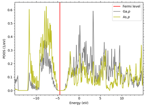 Figure 2. 4p bands of Ga and As in GaAs
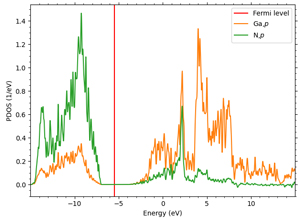 Figure 3. 4p bands of Ga and 2p bands of N in GaN
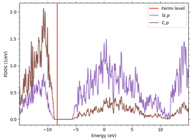 Figure 4. 4p band and 2p band of Si and C in SiC
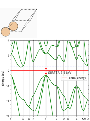 Figure 5. Si: Indirect transition type Experimental value 1.12eV
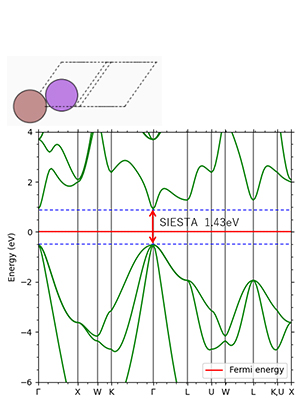 Figure 6. GaAs: direct transition type Experimental value 1.42 eV
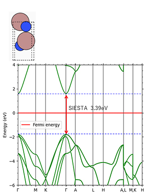 Figure 7.GaN: direct transition type Experimental value 3.39 eV
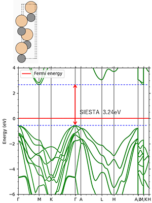 Figure 8. 4H-SiC: Indirect transition type Experimental value 3.26eV